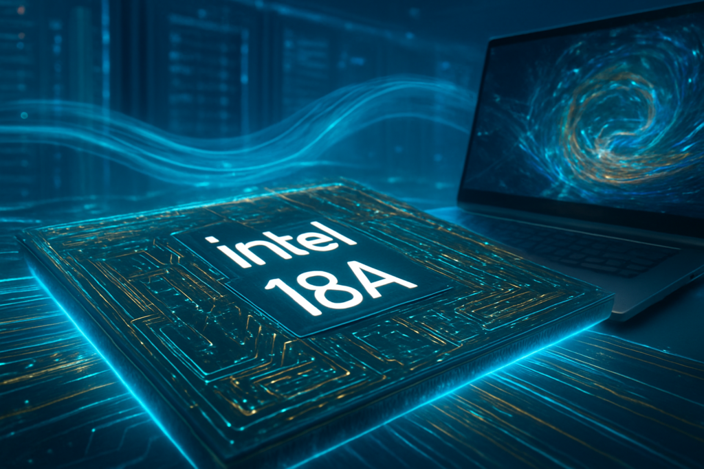
Intel (NASDAQ: INTC) has officially declared victory in its most ambitious engineering campaign to date, announcing today, January 30, 2026, that its Intel 18A process node has entered high-volume manufacturing (HVM). This milestone marks the formal completion of the company’s "5 Nodes in 4 Years" (5N4Y) roadmap, a high-stakes strategy initiated by CEO Pat Gelsinger in 2021 to restore the company to the vanguard of semiconductor manufacturing. With the commencement of HVM for the "Panther Lake" mobile processors and "Clearwater Forest" server chips, Intel has not only met its self-imposed deadline but has also effectively leapfrogged its rivals in several key architectural transitions.
The successful ramp of 18A represents a seismic shift for the global technology sector. By reaching this stage, Intel has validated its move toward a "foundry-first" business model, aimed at challenging the dominance of Taiwan Semiconductor Manufacturing Company (NYSE: TSM). The transition is already bearing fruit, with the company securing significant design wins from hyperscale giants and defense agencies. As the industry grapples with the escalating demands of generative AI, the 18A node provides the dense, power-efficient foundation required for the next generation of neural processing units (NPUs) and massive multi-core data center architectures.
The Technical Triumph of 18A: RibbonFET and PowerVia
The Intel 18A node is more than just a reduction in feature size; it introduces two fundamental architectural changes that the industry has not seen in over a decade. The first is RibbonFET, Intel’s implementation of Gate-All-Around (GAA) transistor technology. Unlike the FinFET transistors used since 2011, RibbonFET wraps the gate entirely around the transistor channel on all four sides. This allows for superior electrical control, significantly reducing current leakage while enabling higher drive currents. In practical terms, 18A offers approximately a 15% improvement in performance-per-watt over the preceding Intel 3 node, allowing chips to run faster without exceeding thermal limits.
Equally revolutionary is PowerVia, Intel's proprietary backside power delivery system. Historically, power and signal wires were layered together on top of the silicon, creating a "spaghetti" of interconnects that led to electrical interference and power loss. PowerVia moves the power delivery circuitry to the reverse side of the wafer, separating it entirely from the signal lines. This architectural shift reduces "voltage droop" (IR drop) by up to 30%, which translates directly into a 6% boost in clock frequency or a significant reduction in power consumption. By clearing the congestion on the top of the die, Intel has also managed to increase transistor density by nearly 10% compared to traditional routing methods.
The dual-pronged launch of Panther Lake and Clearwater Forest showcases these technologies in action. Panther Lake, the new flagship for the Core Ultra Series 3, features the "Cougar Cove" performance cores and the "Darkmont" efficiency cores, alongside a third-generation Xe3 integrated GPU. Notably, it includes an NPU 5 capable of delivering over 50 TOPS (Trillions of Operations Per Second), setting a new bar for on-device AI in thin-and-light laptops. Meanwhile, Clearwater Forest targets the cloud, featuring up to 288 E-cores per socket. It utilizes 18A compute dies stacked onto Intel 3 base tiles using Foveros Direct 3D packaging, a testament to Intel's growing prowess in advanced heterogeneous integration.
A New Competitive Reality for Foundry Giants
The success of 18A has fundamentally altered the competitive landscape between Intel, TSMC, and Samsung (KRX: 005930). While TSMC still maintains a slight edge in raw transistor density, Intel has claimed a significant "first-mover" advantage in backside power delivery. TSMC’s equivalent technology, known as Super Power Rail, is not expected to reach high-volume production until its A16 node in late 2026. This window of technical leadership has allowed Intel to secure "whale" customers that previously relied solely on Asian foundries.
The immediate beneficiaries are tech giants looking to reduce their dependence on a single source of supply. Microsoft (NASDAQ: MSFT) has confirmed that its next-generation Maia AI accelerators will be built on 18A, while Amazon (NASDAQ: AMZN) is utilizing the node for its custom AI fabric chips. Other confirmed partners include Ericsson for 5G infrastructure and Faraday Technology for a 64-core Arm-based SoC. Even companies like NVIDIA (NASDAQ: NVDA) and Broadcom (NASDAQ: AVGO), which have traditionally been loyal to TSMC, are reportedly in active testing phases with 18A. Though Broadcom expressed initial concerns regarding yields in 2025, Intel’s report of 55–75% yield rates in early 2026 suggests the process has matured enough to support high-volume commercial contracts.
For the broader market, Intel’s resurgence provides a much-needed strategic alternative. The concentration of leading-edge logic manufacturing in Taiwan has long been a point of geopolitical concern. With Intel's 18A reaching maturity in its Oregon and Arizona facilities, the "silicon shield" is effectively expanding to North America. This geographic diversification is a strategic advantage for firms like Apple (NASDAQ: AAPL), which is rumored to be qualifying an enhanced 18A-P variant for its 2027 product lineup.
Geopolitical and Historical Significance in the AI Era
The completion of the "5 Nodes in 4 Years" plan is likely to be remembered as one of the most significant turnarounds in industrial history. It marks the end of an era where Intel was often viewed as a "stumbling giant" that had lost its way during the transition to Extreme Ultraviolet (EUV) lithography. By successfully navigating the technical hurdles of 18A, Intel has validated that Moore's Law is not dead but has simply moved into a more complex, three-dimensional phase. This milestone is comparable to the 2011 introduction of the FinFET, which sustained the industry for the last 15 years.
Furthermore, the 18A launch is intrinsically tied to the "AI Gold Rush." As generative AI shifts from massive data centers to local "Edge AI" devices, the performance-per-watt gains of RibbonFET and PowerVia become critical. Without these architectural improvements, the power requirements for running large language models (LLMs) on mobile devices would be prohibitive. Intel’s ability to mass-produce these chips domestically also aligns with the goals of the U.S. CHIPS and Science Act, providing a secure, leading-edge manufacturing base for the U.S. Department of Defense (DoD), which is already a confirmed 18A customer through the RAMP-C program.
However, challenges remain. The massive capital expenditure required to build these "Mega-Fabs" has put significant pressure on Intel’s margins. While the technology is a success, the financial sustainability of the foundry business depends on maintaining high utilization rates from external customers. The industry is watching closely to see if Intel can sustain this momentum without the "heroic" engineering efforts that defined the 5N4Y sprint.
The Road Ahead: 14A and High-NA EUV
Looking toward the future, Intel is already preparing its next major leap: the Intel 14A node. While 18A is the current state-of-the-art, 14A is being designed as the "war node" that Intel hopes will secure undisputed leadership through the end of the decade. This upcoming process will be the first to fully integrate High-NA EUV (High Numerical Aperture) lithography, utilizing the advanced ASML (NASDAQ: ASML) systems that Intel was the first in the industry to acquire.
Near-term developments include the release of the Process Design Kit (PDK) 0.5 for 14A in early 2026, allowing designers to begin mapping out 1.4nm-class chips. We can also expect to see the introduction of PowerDirect, an evolutionary step beyond PowerVia that further optimizes power delivery. Intel has signaled a more disciplined "customer-first" approach for 14A, stating it will only expand capacity once firm commitments are signed, a move meant to appease investors worried about over-expansion.
A Defining Moment for the Semiconductor Industry
The successful launch of 18A and the completion of the 5N4Y roadmap represent a pivotal "mission accomplished" moment for Intel. The company has moved from a position of technical obsolescence to a position where it is defining the industry’s architectural standards for the next decade. The immediate rollout of Panther Lake and Clearwater Forest provides a tangible proof of concept that the technology is ready for prime time.
As we look toward the rest of 2026, the key metrics to watch will be the "foundry ramp"—specifically, whether more high-volume customers like MediaTek or Apple formally commit to 18A production. The technical victory is won; the commercial victory is the next frontier. Intel has successfully rebuilt its engine while flying the plane, and for the first time in years, the company is no longer chasing the leaders of the semiconductor world—it is standing right beside them.
This content is intended for informational purposes only and represents analysis of current AI developments.
TokenRing AI delivers enterprise-grade solutions for multi-agent AI workflow orchestration, AI-powered development tools, and seamless remote collaboration platforms.
For more information, visit https://www.tokenring.ai/.