As of early 2026, the semiconductor industry has reached a definitive turning point where the traditional method of scaling—simply making transistors smaller—is no longer the primary driver of computing power. Instead, the focus has shifted to "Advanced Packaging," a sophisticated method of stacking and connecting multiple chips to act as a single, massive processor. At the heart of this revolution is Taiwan Semiconductor Manufacturing Company (NYSE: TSM), whose System on Integrated Chips (SoIC) technology has become the industry standard for bridging the gap between theoretical chip designs and the massive computational demands of generative AI.
The move to 6-micrometer (6µm) bond pitches represents the current "Goldilocks" zone of semiconductor manufacturing, providing the density required for next-generation AI accelerators like NVIDIA’s (NASDAQ: NVDA) upcoming Rubin architecture and AMD’s (NASDAQ: AMD) Instinct MI400 series. By utilizing hybrid bonding—a process that replaces traditional solder bumps with direct copper-to-copper connections—manufacturers are successfully bypassing the physical limits of monolithic silicon, effectively keeping Moore’s Law alive through vertical integration rather than horizontal shrinkage.
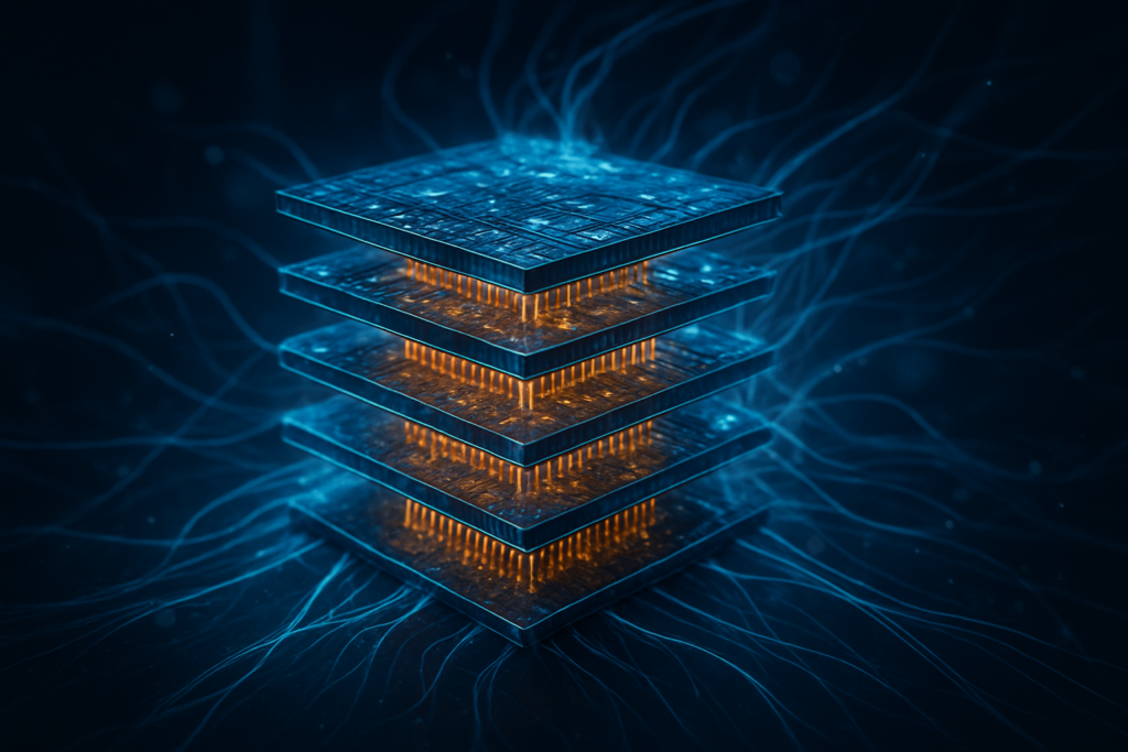
The Technical Frontier: SoIC and the 6µm Milestone
TSMC’s SoIC technology represents the pinnacle of 3D heterogeneous integration, specifically through its "bumpless" hybrid bonding technique known as SoIC-X. Unlike traditional 2.5D packaging, which places chips side-by-side on a silicon interposer (such as CoWoS), SoIC-X allows for logic-on-logic stacking. By reducing the bond pitch—the distance between interconnects—to 6 micrometers, TSMC has achieved a 100x increase in interconnect density compared to the 30-40µm pitches used in traditional micro-bump technologies. This leap allows for massive bandwidth between stacked dies, essentially eliminating the latency that usually occurs when data travels between different parts of a processor.
Technical specifications for the 2026 roadmap indicate that while 6µm is the current high-volume standard, the industry is already testing 4µm and 3µm pitches for late 2026 deployments. This roadmap is critical for the integration of HBM4 (High Bandwidth Memory), which requires these ultra-fine pitches to manage the thermal and electrical signaling of 16-high memory stacks. Initial reactions from the research community have been overwhelmingly positive, with engineers noting that 6µm hybrid bonding allows them to treat separate chiplets as a single "virtual monolithic" die, granting the architectural freedom to mix and match different process nodes (e.g., a 2nm compute die on a 5nm I/O die).
Market Dynamics: The Battle for AI Supremacy
The shift toward high-density hybrid bonding has ignited a fierce competitive landscape among chip designers and foundries. NVIDIA (NASDAQ: NVDA) has pivoted its roadmap to take full advantage of TSMC’s SoIC, moving away from the side-by-side Blackwell designs toward the fully 3D-stacked Rubin platform. This move solidifies NVIDIA’s market positioning by allowing it to pack significantly more compute power into the same physical footprint, a necessity for the power-constrained environments of modern data centers. Meanwhile, AMD (NASDAQ: AMD) continues to leverage its early-mover advantage in 3D stacking; having pioneered SoIC with the MI300, it is now utilizing 6µm bonding in the MI400 to maintain its lead in memory capacity and bandwidth.
However, TSMC is not the only player in this space. Intel (NASDAQ: INTC) is aggressively pushing its Foveros Direct 3D technology, which aims for sub-5µm pitches to support its 18A-PT process node. Intel’s "Clearwater Forest" Xeon processors are the first major test of this technology, positioning the company as a viable alternative for AI companies looking to diversify their supply chains. Samsung (KRX: 005930) is also a major contender with its X-Cube and SAINT platforms. Samsung's unique strategic advantage lies in its "turnkey" capability: it is currently the only company that can manufacture the HBM memory, the logic dies, and the advanced 3D packaging under one roof, potentially lowering costs for hyperscalers like Google or Meta.
Wider Significance: A New Paradigm for Moore’s Law
The wider significance of 6µm hybrid bonding cannot be overstated; it represents the shift from the "Era of Shrink" to the "Era of Integration." For decades, Moore's Law relied on the ability to double transistor density on a single piece of silicon every two years. As that process has become exponentially more expensive and physically difficult, advanced packaging has stepped in as the "Silicon Lego" solution. By stacking chips vertically, designers can continue to increase transistor counts without the catastrophic yield losses associated with building giant, monolithic chips.
This development also addresses the "memory wall"—the bottleneck where processor speed outpaces the speed at which data can be fetched from memory. 3D stacking places memory directly on top of the logic, reducing the distance data must travel and significantly lowering power consumption. However, this transition brings new concerns, primarily regarding thermal management. Stacking high-performance logic dies creates "heat sandwiches" that require innovative cooling solutions, such as microfluidic cooling or advanced diamond-based thermal spreaders, to prevent the chips from throttling or failing.
The Horizon: Glass Substrates and Sub-3µm Pitches
Looking ahead, the industry is already identifying the next hurdles beyond 6µm bonding. The next two to three years will likely see the adoption of glass substrates to replace traditional organic materials. Glass offers superior flatness and thermal stability, which is essential as bond pitches continue to shrink toward 2µm and 1µm. Experts predict that by 2028, we will see the first "3.5D" architectures in the wild—complex systems where multiple 3D-stacked logic towers are interconnected on a glass interposer, providing a level of complexity that was unimaginable a decade ago.
The challenges remaining are primarily economic and logistical. The equipment required for hybrid bonding, such as high-precision wafer-to-wafer aligners, is currently in short supply, and the "cleanliness" requirements for a 6µm bond are far stricter than for traditional packaging. Any microscopic dust particle can ruin a hybrid bond, leading to lower yields. As the industry moves toward these finer pitches, the role of automated inspection and AI-driven quality control will become just as important as the bonding technology itself.
Conclusion: The 3D Future of Artificial Intelligence
The transition to 6-micrometer hybrid bonding and TSMC’s SoIC platform marks a definitive end to the "monolithic era" of computing. As of January 30, 2026, the success of the world’s most powerful AI models is now inextricably linked to the success of 3D vertical stacking. By allowing for unprecedented interconnect density and bandwidth, advanced packaging has provided the industry with a second wind, ensuring that the computational gains required for the next phase of AI development remain achievable.
In the coming months, keep a close eye on the production yields of NVIDIA’s Rubin and the initial benchmarks of Intel’s 18A-PT products. These will serve as the litmus test for whether hybrid bonding can be scaled to the volumes required by the insatiable AI market. While the physical limits of the transistor may be in sight, the architectural possibilities of 3D integration are just beginning to be explored. Moore’s Law isn’t dead; it has simply moved into the third dimension.
This content is intended for informational purposes only and represents analysis of current AI developments.
TokenRing AI delivers enterprise-grade solutions for multi-agent AI workflow orchestration, AI-powered development tools, and seamless remote collaboration platforms.
For more information, visit https://www.tokenring.ai/.