The global technological landscape is undergoing a monumental transformation, driven by an unprecedented surge in investment in semiconductor manufacturing plants (fabs) and research and development (R&D) centers. These massive undertakings, costing tens of billions of dollars each, are not merely industrial expansions; they are powerful engines of economic growth, job creation, and strategic innovation, setting the stage for the next era of artificial intelligence. As the world increasingly relies on advanced computing for everything from smartphones to sophisticated AI models, the foundational role of semiconductors has never been more critical, prompting nations and corporations alike to pour resources into building resilient and cutting-edge domestic capabilities.
This global race to build a robust semiconductor ecosystem is generating profound ripple effects across economies worldwide. Beyond the direct creation of high-skill, high-wage jobs within the semiconductor industry, these facilities catalyze an extensive network of supporting industries, from equipment manufacturing and materials science to logistics and advanced education. The strategic importance of these investments, underscored by recent geopolitical shifts and supply chain vulnerabilities, ensures that their impact will be felt for decades, fundamentally altering regional economic landscapes and accelerating the pace of innovation, particularly in the burgeoning field of artificial intelligence.
The Microchip's Macro Impact: A Deep Dive into Semiconductor Innovation
The current wave of investment in semiconductor fabs and R&D centers represents a significant leap forward in technological capability, driven by the insatiable demand for more powerful and efficient chips for AI and high-performance computing. These new facilities are not just about increasing production volume; they are pushing the boundaries of what's technically possible, often focusing on advanced process nodes, novel materials, and sophisticated packaging technologies.
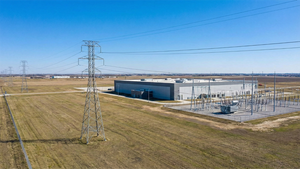
For instance, the Taiwan Semiconductor Manufacturing Company (TSMC) (NYSE: TSM) has committed over $65 billion to build three leading-edge fabs in Arizona, with plans for up to six fabs, two advanced packaging facilities, and an R&D center. These fabs are designed to produce chips using advanced process technologies like 3nm and potentially 2nm nodes, which are crucial for the next generation of AI accelerators. Similarly, Intel (NASDAQ: INTC) is constructing two semiconductor fabs near Columbus, Ohio, costing around $20 billion, with a long-term vision for a megasite housing up to eight fabs. These facilities are critical for Intel's IDM 2.0 strategy, aiming to regain process leadership and become a major foundry player. These investments include extreme ultraviolet (EUV) lithography, a cutting-edge technology essential for manufacturing chips with features smaller than 7nm, enabling unprecedented transistor density and performance. The National Semiconductor Technology Center (NSTC) in Albany, New York, with an $825 million investment, is also focusing on EUV lithography for advanced nodes, serving as a critical R&D hub.
These new approaches differ significantly from previous generations of manufacturing. Older fabs typically focused on larger process nodes (e.g., 28nm, 14nm), which are still vital for many applications but lack the raw computational power required for modern AI workloads. The current focus on sub-5nm technologies allows for billions more transistors to be packed onto a single chip, leading to exponential increases in processing speed and energy efficiency—factors paramount for training and deploying large language models and complex neural networks. Furthermore, the integration of advanced packaging technologies, such as 3D stacking, allows for heterogeneous integration of different chiplets, optimizing performance and power delivery in ways traditional monolithic designs cannot. Initial reactions from the AI research community and industry experts have been overwhelmingly positive, emphasizing that these investments are foundational for continued AI progress, enabling more sophisticated algorithms and real-time processing capabilities that were previously unattainable. The ability to access these advanced chips domestically also addresses critical supply chain security concerns.
Reshaping the AI Landscape: Corporate Beneficiaries and Competitive Shifts
The massive investments in new chip fabs and R&D centers are poised to profoundly reshape the competitive dynamics within the AI industry, creating clear winners and losers while driving significant strategic shifts among tech giants and startups alike.
Companies at the forefront of AI hardware design, such as NVIDIA (NASDAQ: NVDA), stand to benefit immensely. While NVIDIA primarily designs its GPUs and AI accelerators, the increased domestic and diversified global manufacturing capacity for leading-edge nodes ensures a more stable and potentially more competitive supply chain for their crucial components. This reduces reliance on single-source suppliers and mitigates geopolitical risks, allowing NVIDIA to scale its production of high-demand AI chips like the H100 and upcoming generations more effectively. Similarly, Intel's (NASDAQ: INTC) aggressive fab expansion and foundry services initiative directly challenge TSMC (NYSE: TSM) and Samsung (KRX: 005930), aiming to provide an alternative manufacturing source for AI chip designers, including those developing custom AI ASICs. This increased competition in foundry services could lead to lower costs and faster innovation cycles for AI companies.
The competitive implications extend to major AI labs and cloud providers. Hyperscalers like Amazon (NASDAQ: AMZN), Google (NASDAQ: GOOGL), and Microsoft (NASDAQ: MSFT), which are heavily investing in custom AI chips (e.g., AWS Inferentia/Trainium, Google TPUs, Microsoft Maia/Athena), will find a more robust and geographically diversified manufacturing base for their designs. This strategic advantage allows them to optimize their AI infrastructure, potentially reducing latency and improving the cost-efficiency of their AI services. For startups, access to advanced process nodes, whether through established foundries or emerging players, is crucial. While the cost of designing chips for these nodes remains high, the increased manufacturing capacity could foster a more vibrant ecosystem for specialized AI hardware startups, particularly those focusing on niche applications or novel architectures. This development could disrupt existing products and services that rely on older, less efficient silicon, pushing companies towards faster adoption of cutting-edge hardware to maintain market relevance and competitive edge.
The Wider Significance: A New Era of AI-Driven Prosperity and Geopolitical Shifts
The global surge in semiconductor manufacturing and R&D is far more than an industrial expansion; it represents a fundamental recalibration of global technological power and a pivotal moment for the broader AI landscape. This fits squarely into the overarching trend of AI industrialization, where the theoretical advancements in machine learning are increasingly translated into tangible, real-world applications requiring immense computational horsepower.
The impacts are multi-faceted. Economically, these investments are projected to create hundreds of thousands of jobs, both direct and indirect, with a significant multiplier effect on regional GDPs. Regions like Arizona, Ohio, and Texas are rapidly transforming into "Silicon Deserts," attracting a cascade of ancillary businesses, skilled labor, and educational investments. Geopolitically, the drive for domestic chip production, exemplified by initiatives like the U.S. CHIPS Act and the European Chips Act, is a direct response to supply chain vulnerabilities exposed during the pandemic and heightened geopolitical tensions. This push for "chip sovereignty" aims to secure national interests, reduce reliance on single geographic regions for critical technology, and ensure uninterrupted access to the foundational components of modern defense and economic infrastructure. However, potential concerns exist, including the immense capital expenditure required, the environmental impact of energy-intensive fabs, and the projected shortfall of skilled labor, which could hinder the full realization of these investments. Comparisons to previous AI milestones, such as the rise of deep learning or the advent of transformers, highlight that while algorithmic breakthroughs capture headlines, the underlying hardware infrastructure is equally critical. This current wave of semiconductor investment is the physical manifestation of the AI revolution, providing the bedrock upon which future AI breakthroughs will be built.
Charting the Future: What Lies Ahead for Semiconductor Innovation and AI
The current wave of investment in chip fabs and R&D centers sets the stage for a dynamic future, promising both near-term advancements and long-term transformations in the AI landscape. Expected near-term developments include the ramp-up of production at new facilities, leading to increased availability of advanced nodes (e.g., 3nm, 2nm) and potentially easing the supply constraints that have plagued the industry. We will also see continued refinement of advanced packaging technologies, such as chiplets and 3D stacking, which will become increasingly crucial for integrating diverse functionalities and optimizing performance for specialized AI workloads.
Looking further ahead, the focus will intensify on novel computing architectures beyond traditional Von Neumann designs. This includes significant R&D into neuromorphic computing, quantum computing, and in-memory computing, all of which aim to overcome the limitations of current silicon architectures for specific AI tasks. These future developments hold the promise of vastly more energy-efficient and powerful AI systems, enabling applications currently beyond our reach. Potential applications and use cases on the horizon include truly autonomous AI systems capable of complex reasoning, personalized medicine driven by AI at the edge, and hyper-realistic simulations for scientific discovery and entertainment. However, significant challenges need to be addressed, including the escalating costs of R&D and manufacturing for ever-smaller nodes, the development of new materials to sustain Moore's Law, and crucially, addressing the severe global shortage of skilled semiconductor engineers and technicians. Experts predict a continued arms race in semiconductor technology, with nations and companies vying for leadership, and a symbiotic relationship where AI itself will be increasingly used to design and optimize future chips, accelerating the cycle of innovation.
A New Foundation for the AI Era: Key Takeaways and Future Watch
The monumental global investment in new semiconductor fabrication plants and R&D centers marks a pivotal moment in technological history, laying a robust foundation for the accelerated advancement of artificial intelligence. The key takeaway is clear: the future of AI is inextricably linked to the underlying hardware, and the world is now aggressively building the infrastructure necessary to power the next generation of intelligent systems. These investments are not just about manufacturing; they represent a strategic imperative to secure technological sovereignty, drive economic prosperity through job creation and regional development, and foster an environment ripe for unprecedented innovation.
This development's significance in AI history cannot be overstated. Just as the internet required vast networking infrastructure, and cloud computing necessitated massive data centers, the era of pervasive AI demands a foundational shift in semiconductor manufacturing capabilities. The ability to produce cutting-edge chips at scale, with advanced process nodes and packaging, will unlock new frontiers in AI research and application, enabling more complex models, faster processing, and greater energy efficiency. Without this hardware revolution, many of the theoretical advancements in machine learning would remain confined to academic papers rather than transforming industries and daily life.
In the coming weeks and months, watch for announcements regarding the operationalization of these new fabs, updates on workforce development initiatives to address the talent gap, and further strategic partnerships between chip manufacturers, AI companies, and governments. The long-term impact will be a more resilient, diversified, and innovative global semiconductor supply chain, directly translating into more powerful, accessible, and transformative AI technologies. The silicon surge is not just building chips; it's building the future.
This content is intended for informational purposes only and represents analysis of current AI developments.
TokenRing AI delivers enterprise-grade solutions for multi-agent AI workflow orchestration, AI-powered development tools, and seamless remote collaboration platforms.
For more information, visit https://www.tokenring.ai/.