The semiconductor industry has officially entered an era of unprecedented capital expansion, with global equipment spending now projected to reach a record-breaking $156 billion by 2027. According to the latest year-end data from SEMI, the trade association representing the global electronics manufacturing supply chain, this massive surge is fueled by a relentless demand for AI-optimized infrastructure. This isn't merely a cyclical uptick in chip production; it represents a foundational shift in how the world builds and deploys computing power, moving away from the general-purpose paradigms of the last four decades toward a highly specialized, AI-centric architecture.
As of December 19, 2025, the industry is witnessing a "triple threat" of technological shifts: the transition to sub-2nm process nodes, the explosion of High-Bandwidth Memory (HBM), and the critical role of advanced packaging. These factors have compressed a decade's worth of infrastructure evolution into a three-year window. This capital supercycle is not just about making more chips; it is about rebuilding the entire computing stack from the silicon up to accommodate the massive data throughput requirements of trillion-parameter generative AI models.
The End of the Von Neumann Era: Building the AI-First Stack
The technical catalyst for this $156 billion spending spree is the "structural re-architecture" of the computing stack. For decades, the industry followed the von Neumann architecture, where the central processing unit (CPU) and memory were distinct entities. However, the data-intensive nature of modern AI has rendered this model inefficient, creating a "memory wall" that bottlenecks performance. To solve this, the industry is pivoting toward accelerated computing, where the GPU—led by NVIDIA (NASDAQ: NVDA)—and specialized AI accelerators have replaced the CPU as the primary engine of the data center.
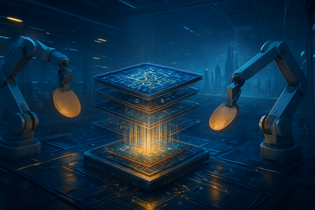
This re-architecture is physically manifesting through 3D integrated circuits (3D IC) and advanced packaging techniques like Chip-on-Wafer-on-Substrate (CoWoS). By stacking HBM4 memory directly onto the logic die, manufacturers are reducing the physical distance data must travel, drastically lowering latency and power consumption. Furthermore, the industry is moving toward "domain-specific silicon," where hyperscalers like Alphabet Inc. (NASDAQ: GOOGL) and Amazon (NASDAQ: AMZN) design custom chips tailored for specific neural network architectures. This shift requires a new class of fabrication equipment capable of handling heterogeneous integration—mixing and matching different "chiplets" on a single substrate to optimize performance.
Initial reactions from the AI research community suggest that this hardware revolution is the only way to sustain the current trajectory of model scaling. Experts note that without these advancements in HBM and advanced packaging, the energy costs of training next-generation models would become economically and environmentally unsustainable. The introduction of High-NA EUV lithography by ASML (NASDAQ: ASML) is also a critical piece of this puzzle, allowing for the precise patterning required for the 1.4nm and 2nm nodes that will dominate the 2027 landscape.
Market Dominance and the "Foundry 2.0" Model
The financial implications of this expansion are reshaping the competitive landscape of the tech world. TSMC (NYSE: TSM) remains the indispensable titan of this era, effectively acting as the "world’s foundry" for AI. Its aggressive expansion of CoWoS capacity—expected to triple by 2026—has made it the gatekeeper of AI hardware availability. Meanwhile, Intel (NASDAQ: INTC) is attempting a historic pivot with its Intel Foundry Services, aiming to capture a significant share of the U.S.-based leading-edge capacity by 2027 through its "5 nodes in 4 years" strategy.
The traditional "fabless" model is also evolving into what analysts call "Foundry 2.0." In this new paradigm, the relationship between the chip designer and the manufacturer is more integrated than ever. Companies like Broadcom (NASDAQ: AVGO) and Marvell (NASDAQ: MRVL) are benefiting immensely as they provide the essential interconnect and custom silicon expertise that bridges the gap between raw compute power and usable data center systems. The surge in CapEx also provides a massive tailwind for equipment giants like Applied Materials (NASDAQ: AMAT), whose tools are essential for the complex material engineering required for Gate-All-Around (GAA) transistors.
However, this capital expansion creates a high barrier to entry. Startups are increasingly finding it difficult to compete at the hardware level, leading to a consolidation of power among a few "AI Sovereigns." For tech giants, the strategic advantage lies in their ability to secure long-term supply agreements for HBM and advanced packaging slots. Samsung (KRX: 005930) and Micron (NASDAQ: MU) are currently locked in a fierce battle to dominate the HBM4 market, as the memory component of an AI server now accounts for a significantly larger portion of the total bill of materials than in the previous decade.
A Geopolitical and Technological Milestone
The $156 billion projection marks a milestone that transcends corporate balance sheets; it is a reflection of the new "silicon diplomacy." The concentration of capital spending is heavily influenced by national security interests, with the U.S. CHIPS Act and similar initiatives in Europe and Japan driving a "de-risking" of the supply chain. This has led to the construction of massive new fab complexes in Arizona, Ohio, and Germany, which are scheduled to reach full production capacity by the 2027 target date.
Comparatively, this expansion dwarfs the previous "mobile revolution" and the "internet boom" in terms of capital intensity. While those eras focused on connectivity and consumer access, the current era is focused on intelligence synthesis. The concern among some economists is the potential for "over-capacity" if the software side of the AI market fails to generate the expected returns. However, proponents argue that the structural shift toward AI is permanent, and the infrastructure being built today will serve as the backbone for the next 20 years of global economic productivity.
The environmental impact of this expansion is also a point of intense discussion. The move toward 2nm and 1.4nm nodes is driven as much by energy efficiency as it is by raw speed. As data centers consume an ever-increasing share of the global power grid, the semiconductor industry’s ability to deliver "more compute per watt" is becoming the most critical metric for the success of the AI transition.
The Road to 2027: What Lies Ahead
Looking toward 2027, the industry is preparing for the mass adoption of "optical interconnects," which will replace copper wiring with light-based data transmission between chips. This will be the next major step in the re-architecture of the stack, allowing for data center-scale computers that act as a single, massive processor. We also expect to see the first commercial applications of "backside power delivery," a technique that moves power lines to the back of the silicon wafer to reduce interference and improve performance.
The primary challenge remains the talent gap. Building and operating the sophisticated equipment required for sub-2nm manufacturing requires a workforce that does not yet exist at the necessary scale. Furthermore, the supply chain for specialty chemicals and rare-earth materials remains fragile. Experts predict that the next two years will see a series of strategic acquisitions as major players look to vertically integrate their supply chains to mitigate these risks.
Summary of a New Industrial Era
The projected $156 billion in semiconductor capital spending by 2027 is a clear signal that the AI revolution is no longer just a software story—it is a massive industrial undertaking. The structural re-architecture of the computing stack, moving from CPU-centric designs to integrated, accelerated systems, is the most significant change in computer science in nearly half a century.
As we look toward the end of the decade, the key takeaways are clear: the "memory wall" is being dismantled through advanced packaging, the foundry model is becoming more collaborative and system-oriented, and the geopolitical map of chip manufacturing is being redrawn. For investors and industry observers, the coming months will be defined by the successful ramp-up of 2nm production and the first deliveries of High-NA EUV systems. The race to 2027 is on, and the stakes have never been higher.
This content is intended for informational purposes only and represents analysis of current AI developments.
TokenRing AI delivers enterprise-grade solutions for multi-agent AI workflow orchestration, AI-powered development tools, and seamless remote collaboration platforms.
For more information, visit https://www.tokenring.ai/.


